GlobalFoundries Silicon Photonics DoC Funding 2026 Analysis
Neutral, data-driven perspective on GlobalFoundries silicon photonics DoC funding 2026 and implications for U.S. AI infrastructure.

Nil Ni is a seasoned journalist specializing in emerging technologies and innovation. With a keen eye for detail, Nil brings insightful analysis to Stanford Tech Review, enriching readers’ understanding of the tech landscape.
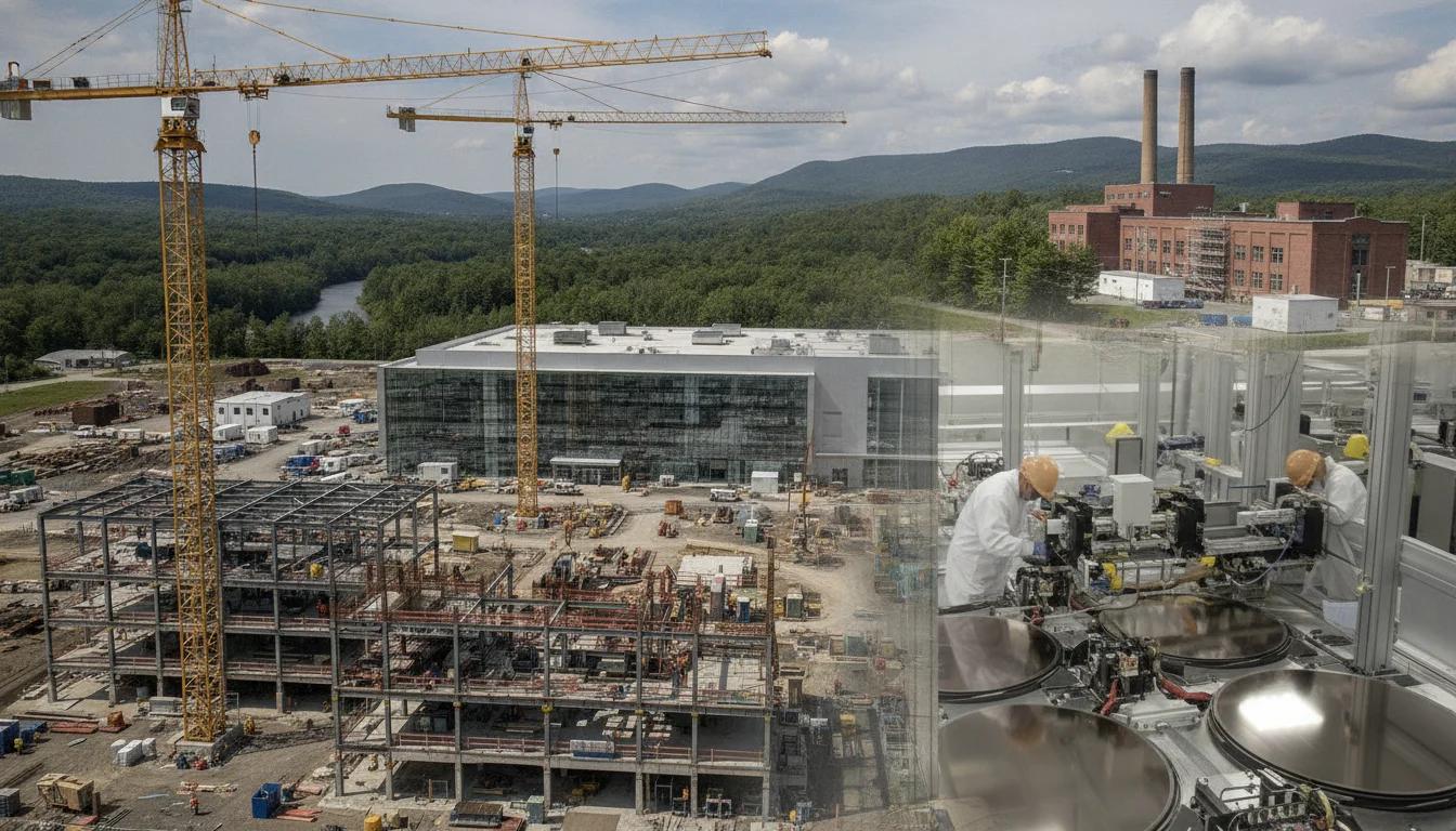
The pace of AI infrastructure innovation hinges not only on software breakthroughs or new chip architectures, but increasingly on the hardware ecosystems that enable them. GlobalFoundries’ recent engagement with the U.S. Department of Commerce over silicon photonics funding for 2026 is a signal flare in a broader policy-and-technology convergence: public incentives shaping private R&D, and private scale enabling national ambitions in computing speed, data center efficiency, and AI capability. The question before readers today is not simply whether a single award will move a technology forward, but how a policy-driven infusion interacts with global supply chain realities, semiconductor manufacturing challenges, and the competitive dynamics of photonics-enabled AI acceleration. GlobalFoundries announced on July 29, 2026 that it had signed a letter of intent with the U.S. Department of Commerce to accelerate next-generation silicon photonics, a $300 million award that would be a foundation for scale and innovation in domestic photonics. This central fact, confirmed by the company’s official release, anchors the analysis that follows. according to GlobalFoundries' press release. (gf.com)
My core thesis is straightforward: this kind of DoC funding is a strategic lever for U.S. leadership in silicon photonics, but it is not a silver bullet. It must be integrated with disciplined R&D programs, practical manufacturing ramp plans, and a coherent market strategy that aligns with the needs of AI data centers, edge computing, and high-performance networking. The broader context—policy incentives under CHIPS and Science Act umbrella, evolving materials and integration platforms, and the competitive landscape with other global photonics players—means we should expect a multi-year, multi-faceted rollout rather than a one-shot boost. The implications extend beyond GlobalFoundries: they illuminate how government funding, corporate R&D priorities, and industry ecosystems interact to shape the next generation of optical data pathways.
Section 1: The Current State
Policy momentum and the CHIPS landscape
The U.S. government has structured incentives to accelerate semiconductor research and development, particularly in areas that promise performance gains for AI, machine learning, and data center workloads. As a backdrop, the Department of Commerce, through the CHIPS and Science Act framework, has signaled a substantial appetite for funding R&D in advanced microelectronics, including silicon photonics and related packaging. In July 2026, the Department of Commerce announced letters of intent with multiple firms to catalyze R&D across compute and communications infrastructures, with billions of dollars in incentives across various projects. This policy environment creates a corridor of opportunity for private companies to pair with federal programs, align on long-horizon research agendas, and de-risk early-stage, high-impact photonics work. The government’s public materials show a deliberate emphasis on integrated photonics, materials, and packaging as critical to America’s compute supply chain resilience. For readers tracking the policy arc, this CHIPS-focused activity provides essential context for why GlobalFoundries and peers pursue formal DoC engagements in 2026. This framing is supported by official releases and independent government analyses. (nist.gov)
In this policy milieu, a $300 million LOI with the U.S. Department of Commerce translates into more than a funding line; it signifies a bridge between national strategy and corporate R&D programs. The CHIPS program has evolved to include direct funding and incentive structures designed to accelerate domestic capabilities in silicon photonics, silicon-germanium, and advanced packaging—precisely the kinds of capabilities GlobalFoundries has been expanding around its Malta, New York, and other U.S. facilities. The formal LOI, while an initial step, sets expectations for milestones, collaboration frameworks, and potential equity considerations as part of the funding arrangement. Photonics industry coverage and official program materials corroborate that this funding track is part of a broader push to de-risk and scale photonics-enabled compute for AI and data centers. (photonics.com)
GlobalFoundries’ silicon photonics strategy and SCALE
GlobalFoundries’ foray into silicon photonics has been anchored by a strategy to integrate optical components closely with silicon-based processing and packaging. The company has highlighted platforms like SCALE (Silicon Photonics Co-Packaged Advanced Light Engine) as a core enabler for near-packaged optics (NPO) and co-packaged optics (CPO) that could deliver higher bandwidth and lower latency for AI workloads. The LOI with the DoC aligns with that strategic focus, signaling government validation and potential acceleration of work on materials, wafer technologies, and packaging innovations that can ultimately scale to commercial data-center deployments. The company’s public disclosures underscore a trajectory toward more integrated photonics architectures that connect optical interconnects with silicon logic and memory, a pathway widely discussed in industry analyses as essential for future AI compute scalability. The dialogue around SCALE and related R&D efforts is echoed in industry reporting and GF’s own notices. (gf.com)
The market context: photonics, AI, and data-center demand
Industry coverage in 2026 consistently spots silicon photonics as a strategic enabler for AI infrastructure—especially for data-center interconnects, high-speed networks, and energy-efficient compute. Independent photonics outlets and technology press have highlighted GlobalFoundries’ involvement in DOC funding and related collaborations as part of a broader trend: governments funding semiconductor R&D to sustain domestic leadership in photonics-enabled compute. Reports describe how photonics, materials science, and advanced packaging converge to reduce energy per operation and increase data throughput, both of which are central to modern AI training and inference pipelines. While not every claim can be quantified in advance of formal program results, the narrative from industry observers aligns with the idea that government-backed photonics R&D can shorten development cycles for next-generation interconnects and optical engines. (photonics.com)
The formal acknowledgement of the funding pathway
Beyond press releases, the CHIPS program and NIST communications around 2026 show a deliberate strategy to allocate incentives for photonics and related areas. The U.S. Department of Commerce’ CHIPS program spurred the signing of multiple letters of intent to provide incentives for R&D across the compute supply chain, which includes optics, materials, and packaging—areas in which GlobalFoundries is actively investing. These official notices are essential for readers who want to track the policy-to-portfolio translation and understand how much of the funding actually translates into tangible, near-term R&D activity on the ground. This official activity is corroborated by government analyses and trade press reporting on the CHIPS incentives rollout. (nist.gov)
A note on timing and expectations
The July 29, 2026 LOI marks an early milestone; it is not a final grant agreement. Later developments—such as definitive awards, procurement cycles, or equity arrangements—will shape the pace and scope of work. The government’s own oversight and the way funds are disbursed can introduce variability in project timing. In the context of silicon photonics, where wafer-level integration, materials science, and packaging innovations interact with fabrication processes and yield challenges, this is a normal feature of large-scale, government-supported R&D programs. The CAUTION here is that readers should interpret LOIs as strategic commitments that may be refined or expanded as projects mature, rather than as instant, cash-on-the-table guarantees. This nuance is reflected in official and industry commentary about CHIPS-oriented funding. (nist.gov)
Section 2: Why I Disagree
The funding signal is not a silver bullet for hardware breakthroughs
A central point of tension in public commentary is the belief that a large DoC award will automatically accelerate silicon photonics breakthroughs. In reality, the path from LOI to deployed, scale-ready technology involves layered steps: continued research, successful demonstrations, supply chain readiness, manufacturing yield improvements, and the bridging of R&D into production lines. Public incentives can meaningfully de-risk early work and catalyze collaboration, but the technical uncertainties in silicon photonics—materials compatibility, waveguide fabrication, optical packaging, and thermal management—remain substantial. The core risk is that a grant award alone does not resolve these technical challenges; the problem is not just capital, but integration capability and timing with manufacturing ecosystems. This perspective is consistent with how government programs operate in practice, where LOIs are followed by multi-year programs with milestones and performance requirements. (nist.gov)
Equity and governance dynamics introduce complexity
GlobalFoundries’ own disclosures have indicated that the DoC engagement could involve equity considerations and governance terms—such as the DoC taking a stake (for example, around 1% in some discussions) as part of the incentives framework. While equity can align incentives and demonstrate government confidence, it also introduces governance complexity and potential constraints on corporate strategies or competitive positioning. Understanding how these governance terms play out is essential for evaluating whether the funding will translate into durable market advantage or create frictions in execution. Reported discussions around equity in connection with CHIPS Act funding provide a cautionary reminder that public-private partnerships carry both strategic upside and administrative complexity. (semiconductorindustrymonthly.com)
The interplay with private sector dynamics and other players
The silicon photonics ecosystem is global and competitive. Partnerships, acquisitions, and collaborations shape the pace of innovation. For instance, GF’s activity around SCALE and related initiatives interacts with other industry players and research organizations. Reports have noted GF engagement with other photonics and packaging efforts, and there are industry accounts of GF’s collaboration strategies and technology moves (including recent deals and consolidation in the photonics space). This competitive context matters because government funding does not operate in isolation; it interacts with corporate decisions about investment priorities, supply chains, and go-to-market timing. The broader market context suggests that while the DOC funding is important, success will hinge on execution across materials, wafer technology, packaging, and system integration, not merely on the size of the grant. (electronics360.globalspec.com)
Technological risk remains high in silicon photonics
Silicon photonics is a field defined by relentless experimentation at the intersection of materials science, nanofabrication, and optical engineering. Transitioning from wafer-scale demonstration to production-grade interconnects and optical engines requires breakthroughs in yield, reliability, and packaging integration. While the DoC funding under CHIPS is designed to address R&D gaps, it cannot substitute for the foundational engineering work that determines whether a photonics solution can scale in real data-center environments. The precaution here is not to be pessimistic, but to recognize that the path from LOI to market-ready silicon photonics systems is non-linear and often longer than public narratives imply. Industry and policy analyses consistently stress the chronic gap between research milestones and production-scale deployment in photonics, which is a crucial reality for any optimistic forecast. (nist.gov)
Section 3: What This Means
Implications for GlobalFoundries and the SCALE roadmap
The LOI and subsequent funding signals a green light for continued investment in silicon photonics platforms such as SCALE, which seek to bridge optical interconnects with silicon-based compute elements. If the DoC funding translates into a multi-year R&D program with clear milestones, GF could accelerate its ability to deliver near-packaged optics and co-packaged optics that improve data-center interconnect bandwidth and energy efficiency. For readers tracking the technology trajectory, this alignment between policy support and platform development suggests that GF’s efforts to push silicon photonics into higher levels of integration may gain priority in budgeting and project planning. Yet the company must deliver tangible results—demonstrations of scalable wafer-level photonics, robust packaging solutions, and integrated optics that align with AI workloads. The interplay between public incentives and private execution will determine whether the SCALE roadmap moves from ambitious concept to practical, high-volume supply. (gf.com)
Policy and industry implications for the broader ecosystem
For policymakers, the GlobalFoundries case illustrates how CHIPS Act incentives can catalyze targeted R&D in strategic technologies. It also underscores the importance of transparent milestones, governance terms, and accountability mechanisms to ensure effective deployment of public funds. For industry players, the case reinforces the value of establishing early, credible collaborations with government programs and aligning technical roadmaps with policy timelines. The NIST and CHIPS program literature, which documents the program’s broad scope and the funding envelope across multiple firms, provides context for other companies evaluating similar partnerships. The result is a more dynamic, policy-aligned photonics ecosystem that can, in principle, deliver faster innovation cycles for AI infrastructure, provided that milestones are clearly defined and met. (nist.gov)
Practical takeaways for practitioners and researchers
- Align research agendas with deployed funding milestones: researchers should map their photonics work to anticipated program milestones, ensuring that deliverables align with the criteria that funding authorities value (materials breakthroughs, packaging innovations, manufacturing readiness, etc.).
- Prepare for longer-term timelines: even with strong funding, silicon photonics progress involves multi-year development cycles, pilot lines, and qualification processes. Communities involved in this ecosystem should set expectations for incremental progress rather than abrupt leaps.
- Emphasize integration capabilities: success will likely hinge on how well optical components integrate with silicon logic, memory, and packaging. Projects that foreground co-design across photonics and electronics will be advantaged.
- Monitor governance and compliance: as public funds flow, oversight, reporting, and equity considerations become part of the operational fabric. Teams should design governance processes that meet both scientific and regulatory expectations. (nist.gov)
Closing
The intersection of policy incentives and private photonics innovation is a crucible for the next phase of AI infrastructure. GlobalFoundries’ DoC funding engagement in 2026 is a meaningful signal that silicon photonics is viewed as a strategic capability for domestic leadership in compute and data-center performance. But as with any large public-private program, the real story will be written in the milestones achieved, the manufacturing realities overcome, and the extent to which this funding translates into scalable, reliable, and affordable silicon photonics solutions for AI workloads. The path ahead will demand disciplined execution, transparent milestones, and a willingness to adjust course as the technology and market evolve. For readers, the key takeaway is simple: this is not just a grant; it is a directional shift that warrants close watch, rigorous analysis, and active engagement from researchers, practitioners, and policymakers alike.
GlobalFoundries’ ongoing R&D ambitions in silicon photonics, as reinforced by the DOC LOI and subsequent funding developments, carry implications that extend far beyond a single award. They illuminate how policy instruments can accelerate strategic technologies and how industry players must navigate the practicalities of bringing advanced photonics from laboratory demonstrations into production-ready, enterprise-scale ecosystems. If the U.S. intends to maintain leadership in AI infrastructure, the coordination between DoC funding, corporate R&D roadmaps, and the broader photonics ecosystem will be essential. The road ahead is long, and progress will be measured not only by the size of awards but by the timeliness and reliability of deliverables that enable faster, more energy-efficient AI at scale. As auditors, skeptics, and technologists, we should demand clarity on milestones, insist on transparent reporting, and recognize that true leadership in silicon photonics will emerge through disciplined collaboration, not grand promises alone.